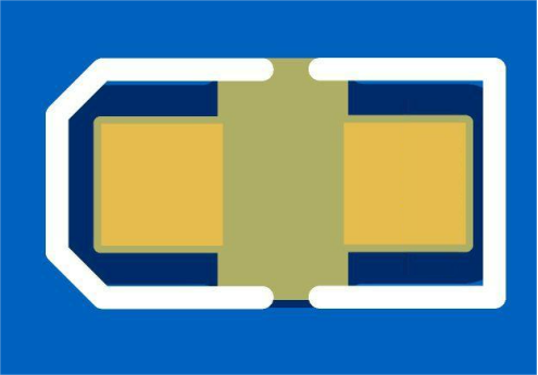
When engaged in PCB design, the integration of indicator lights is a common requirement. However, the luminosity of a front-facing LED can be excessive, impeding the clarity of the displayed information. To address this, a diffusion layer and an accompanying icon can be incorporated for enhanced visual presentation.
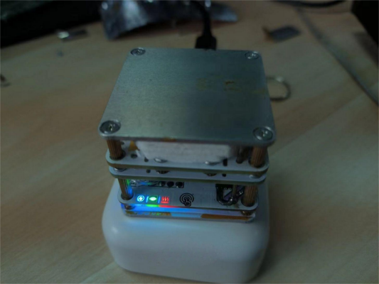
In proximity to the PCB,
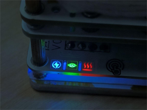
The underlying principle is straightforward: affix LEDs to the back and project the designated pattern onto the front surface through the PCB. Notwithstanding its simplicity, the practical execution of this process demands a nuanced approach.
Step 1: Pattern Selection
Given the inherent limitations in LED brightness, it is imperative to opt for patterns of modest proportions to ensure uniform luminosity. Complexity should be minimized, with preference for straightforward black and white line patterns. Reference can be drawn from commonly utilized web icons.

Step 2: Pattern Refinement
Adjustments, including cropping and sharpening, may be necessary based on the selected pattern. For already clear images, a focused cropping approach suffices. It is essential to align the pattern to one side during cropping to avoid excessive blank spaces.

Step 3: PCB Visualization
Place the image onto the PCB, fine-tuning parameters such as tolerance and smoothness for optimal visual representation. Critical to this process is resizing the image, accounting for width and height. Consideration should be given to the orientation of the pattern during cropping, with adjustments made accordingly. In cases of uncertainty, employ the inverse selection tool to identify changing values and make proportional adjustments.
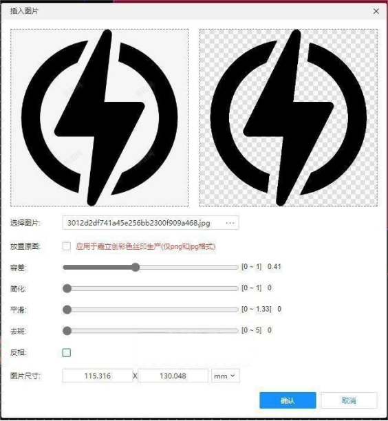
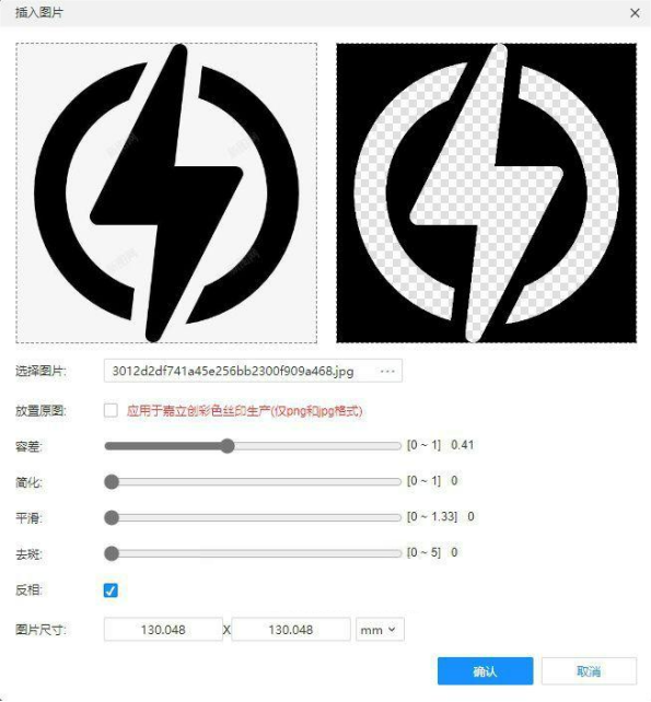
In the illustrative example, focus on adjusting the height value. Initially, place the image with a designated height, confirm, and subsequently transition to the solder mask layer. Repeat the process with the inverse selection, aligning the height accordingly.


Step 4: Rear Placement of LEDs
To prevent copper coverage beneath the LEDs, incorporate a designated no-copper zone and subsequently rebuild the copper. Analogously, adjust to the solder mask layer and introduce a fill in the same spatial configuration.
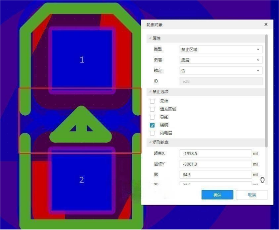
Considerations for potential impact on the area below the LED, specifically the triangular silk print, are paramount. Select the component, right-click, initiate package editing, opt to select only the component, and proceed to delete the silk print beneath the LED, saving the modifications.
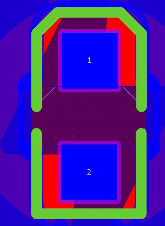
A comprehensive assessment of the final effect can be conducted through a meticulous review of the 3D rendering.

