As societal advancements continue, the landscape of mobile technology has embraced the era of super-fast charging capabilities. Carrying a charger now promises rapid replenishment of battery power within minimal timeframes. In light of these developments, let's embark on a journey to enhance a power bank in tandem with the insights provided in this article.
Procedure:
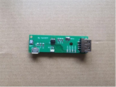
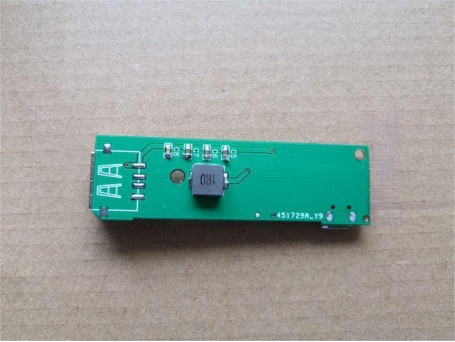
The ubiquitous IP5306 charging module, albeit widely used, presents spatial constraints unsuitable for the intended modifications to the power bank. Thus, meticulous measurements and circuit designs are imperative. The modification process mirrors conventional practices, entailing schematic illustrations, board fabrication, and component assembly, facilitated by tools such as hot air guns and soldering irons.
Outcomes:
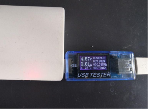
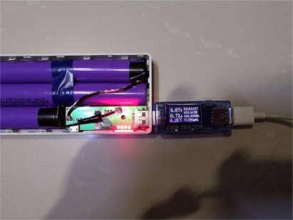
Upon conducting charging trials, a commendable output of 1.85A was observed, albeit slightly below the stipulated 2.1A threshold as per the datasheet, achieving an efficiency rating of 91%. Extrapolating from this data, an anticipated theoretical value of approximately 1.9A is calculated, showcasing promising results. Subsequent discharge assessments may reveal varying performance metrics across devices, underscoring the intricacies of load compatibility and potential battery issues.
Future Prospects:
To further augment the charging capabilities, the integration of a chip compatible with fast charging protocols is a promising avenue. Collaborating with the IP5306, this enhancement could elevate charging efficiency and compatibility. Additionally, exploring alternative charging management chips could unveil novel opportunities for optimization.
Board Prototypes
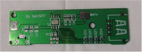
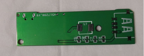
Component Installation, Modification Completion
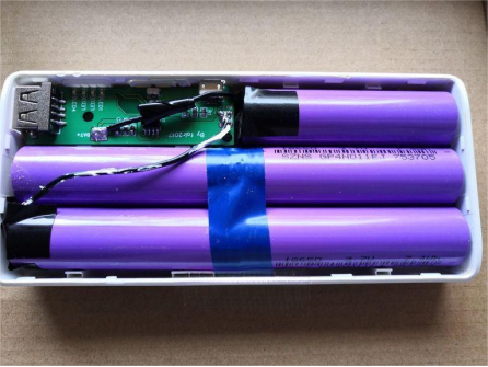
No-load Efficiency Demonstration
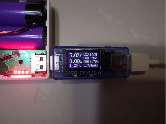
Charging Trial Analysis
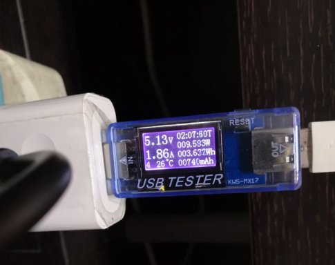
Discharge Evaluation
