On June 12, Samsung Electronics showcased its latest advancements in foundry technology at the annual Samsung Foundry Forum (SFF) held at the Device Solutions America headquarters in San Jose, California.
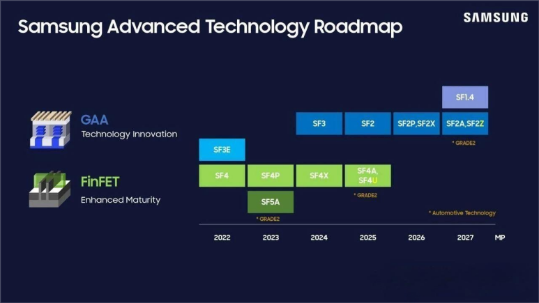
Under the theme "Empowering the AI Revolution," Samsung announced significant enhancements to its process technology roadmap, introducing two cutting-edge nodes—SF2Z and SF4U. Additionally, Samsung presented an integrated AI solutions platform that leverages its expertise in foundry, memory, and advanced packaging (AVP).
Samsung's newest 2nm process, SF2Z, features optimized Backside Power Delivery Network (BSPDN) technology, which positions power rails on the wafer's backside, eliminating bottlenecks between power and signal lines. Compared to the first-generation 2nm node SF2, the SF2Z's application of BSPDN not only improves power, performance, and area (PPA) but also significantly reduces IR drop, enhancing HPC design performance. Mass production of SF2Z is anticipated in 2027.

The SF4U node, a high-value 4nm variant, offers PPA improvements through optical shrink techniques and is expected to enter mass production in 2025.
Samsung also reported that preparations for the SF1.4 (1.4nm) node are advancing smoothly, with performance and yield targets on track for mass production by 2027. Reinforcing its commitment to surpassing Moore's Law, Samsung is actively developing future process technologies below 1.4nm through innovations in materials and structures.
Moreover, Samsung highlighted its Gate-All-Around (GAA) transistor technology, announcing plans to commence mass production of second-generation 3nm chips using GAA in the second half of this year.
Samsung also introduced its AI solutions platform, emphasizing the streamlined communication channels that enable customers to manage interactions with its memory, foundry, and chip packaging teams more efficiently. This integration reduces the typical AI chip production time by approximately 20%.
In addition to advanced process nodes, Samsung offers specialized and 8-inch wafer derivative products, continuously improving PPA with strong cost competitiveness.
Looking ahead, Samsung plans to launch an integrated, CPO-based AI solution in 2027, aiming to provide customers with a comprehensive one-stop AI solution.


