Due to unexpected power outages and the widespread adoption of the PD protocol, I've DIYed a multi-protocol USB-A charging board (IP6505T) with a 24V bus. If you’re interested, feel free to check out this article.
The sub-boards are designed as follows:
· LM5176 (PD100W)
· LM3150 (5V 8A 40W) x2
· IP6505T (24W) x3
· SW3526 (PD65W) + LM25116 (20V 3.25A 65W)
· PL5501 x2 (PD65W)
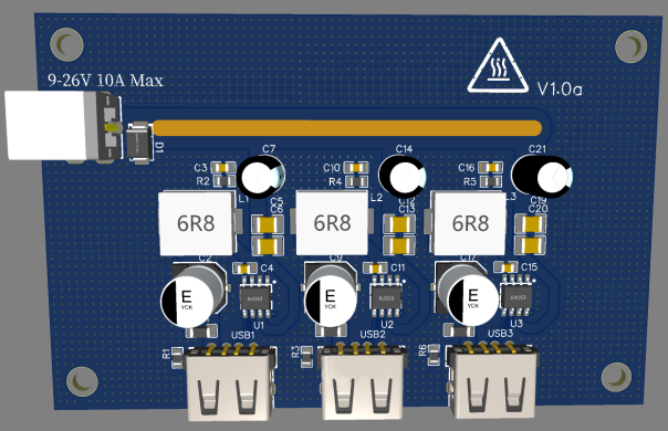
3D Simulation Image:

Chip Overview:
The IP6505T is an integrated synchronous buck converter with built-in power MOSFETs. It accepts an input voltage range of 4.5V to 32V and provides an output voltage range of 3V to 12V, with a maximum output power of 24W. It automatically adjusts the output voltage and current based on the detected fast charging protocol, offering typical outputs of: 4V@3.6A, 5V@3.4A, 7V@3A, 9V@2.5A, and 12V@2A.
With an efficiency of up to 97%, the IP6505T features constant voltage (CV) and constant current (CC) characteristics. When the output current is below the set value, it operates in CV mode with a constant voltage; when the current exceeds the limit, it switches to CC mode, reducing the voltage.
Additionally, the IP6505T has a line compensation feature that increases the output voltage as current rises, compensating for voltage drops caused by cable resistance. It also includes soft start functionality to prevent inrush currents from affecting power supply stability. The chip integrates various fast charging protocols and can automatically recognize supported protocols via DP/DM, adjusting the output voltage and current accordingly.
The IP6505T is equipped with multiple protection features, including input over-voltage, under-voltage, output over-current, over-voltage, under-voltage, and short-circuit protection.
In summary, this car charging IC supports 12V and 24V inputs and integrates multiple USB-A fast charging protocols. However:
It does not support VOOC (the IP6505T-Pro does).
The integrated SCP protocol has been blocked by newer versions of "Wow" smartphones.
Supported Fast Charging Protocols:
· BC1.2, Apple, Samsung Protocol (5V)
· Qualcomm QC2.0 and QC3.0 (Certification No.: 4788120153-2)
· MTK PE1.1/PE2.0
· Huawei Fast Charge Protocol FCP
· Huawei Fast Charge Protocol SCP
· Samsung Fast Charge Protocol AFC
· Spreadtrum Fast Charge Protocol SFCP
Schematic: (Three identical paths, shown for one)

· C5, C6: Input MLCC filter capacitors
· C7: Input solid-state filter capacitor
· R2, C3: SW node damping circuit to absorb spikes and improve EMC performance
· C4: Bootstrap capacitor for NMOS driver
· C1: Output MLCC filter capacitor
· C2: Output aluminum electrolytic filter capacitor
· R1: Output discharge resistor
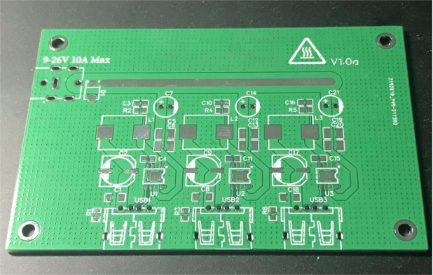
PCB Fabrication

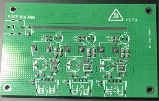
Apply Solder Paste:

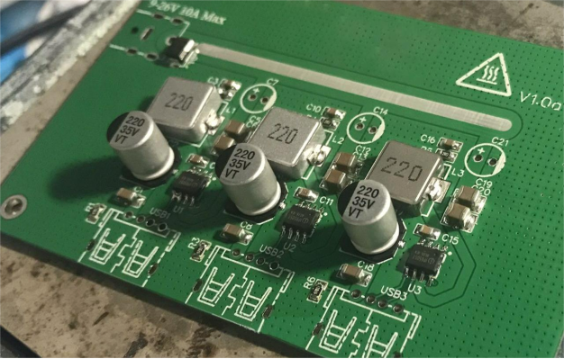
Place Surface-Mount Components:

Preheat the hot plate, then place the board on it, using tweezers to align the components.

Keeping all components on the front side offers two major benefits:
1.Easier soldering; the hot plate can complete it in just a minute.
2.No need to worry about conflicts with the components on the underside when stacked.
Next, touch up the solder connections with a soldering iron and attach the through-hole components:

Power On for Testing: Static current is 6mA at 24V. Testing the fast charging protocols:

Charge a Power Bank:

Ripple is a bit high, reaching 120mV. If this concerns you, consider adding a few more MLCCs to see the effect.
All done!


