
Lightmatter Guide DR, 3D Silicon Photonics Push with TSMC


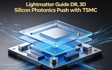
According to industry developments, the rapid growth of AI computing workloads is placing unprecedented demands on data center infrastructure, making interconnect technologies and laser-based photonics critical for overcoming bandwidth and power efficiency bottlenecks. Silicon photonics unicorn Lightmatter has recently introduced its latest laser product, Guide DR, featuring an innovative Laser Network Interface Card (LNIC) form factor designed to deliver a new architecture for high-density laser light sources. At the same time, the company is deepening collaboration with TSMC on a Compact Universal Photonic Engine (COUPE) platform, aiming to advance the development of 3D-stacked silicon photonic engines.
Founded in 2017 by a research team from the Massachusetts Institute of Technology (MIT), Lightmatter has raised approximately $850 million in funding and reached a valuation of around $4.4 billion. CEO Nick Harris stated that the company’s core product families are Passage and Guide. Among them, Passage L20 is recognized as the world’s first Near-Packaged Optics (NPO) solution using bidirectional (BiDi) technology. By integrating transmit and receive functions into a single optical fiber, it can reduce AI data center networking costs by up to 16%.
According to Lightmatter’s technology roadmap, Near-Packaged Optics (NPO) is expected to begin deployment in 2027, while Co-Packaged Optics (CPO) technology is targeted for introduction in 2028, followed by interposer-based architectures after 2029.
The Guide product line represents Lightmatter’s laser technology portfolio. Harris compared the role of lasers in optical communications to battery systems in electric vehicles, emphasizing their foundational importance. In January 2026, the company unveiled the world’s first Very Large-Scale Photonics (VLSP) laser chip, capable of integrating up to 128 laser diodes on a single chip. Unlike traditional indium phosphide (InP)-based laser manufacturing, the Guide series combines InP with 300mm CMOS wafer processes, significantly reducing InP material usage and lowering reliance on the conventional InP supply chain.
On May 22, Lightmatter officially launched Guide DR in Mountain View, California. The product adopts the LNIC form factor and is designed to fully leverage existing liquid-cooling infrastructure. Compared with traditional external laser small form-factor pluggable modules (ELSFP), it can increase per-rack density by approximately four times and scale up to clusters of up to 1,000 XPUs.
Harris noted that 2027 will be a pivotal growth phase for the Guide laser product line. Assuming stable supply chain and manufacturing capacity, Lightmatter plans to focus on hyperscale cloud service providers and ASIC customers to expand its market presence.
To support the massive computing demand driven by AI applications, Lightmatter is collaborating with multiple semiconductor foundries, including GlobalFoundries and Tower Semiconductor, alongside TSMC. Harris disclosed that several co-developed products with TSMC are expected to enter production around 2027. TSMC has previously announced that its COUPE-based 200Gbps microring modulator (MRM) technology is scheduled for mass production in 2026. He emphasized that TSMC’s COUPE platform offers significant advantages and represents a critical enabling technology for hyperscale cloud infrastructure. Lightmatter also maintains long-term collaboration with TSMC in advanced 3D packaging technologies.
Regarding the challenges of CPO deployment, Harris highlighted that validation and rack-level system design remain the primary barriers to large-scale commercialization. The company is currently working closely with Dell Technologies, Quanta, and Celestica to define next-generation CPO rack standards and has already submitted the first revision of its rack design to the Open Compute Project (OCP).


