
Samsung Begins HBM Expansion at Onyang Plant in 2026


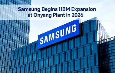
According to reports, Samsung Electronics plans to begin expanding its semiconductor packaging facility in Onyang, South Korea, in October 2026 with an investment of KRW 1.3 trillion (approximately USD 884 million). The project is designed to strengthen the company's advanced packaging capabilities and support mass production of High Bandwidth Memory (HBM) by May 2029.
Samsung Electronics and Asan City, located in South Korea's Chungcheong Province, signed a memorandum of understanding (MOU) on July 22 to support the expansion project. The agreement outlines administrative cooperation and local development measures aimed at facilitating construction while contributing to regional economic growth.
The new facility will feature a 31,000-square-meter cleanroom—roughly equivalent to the size of four football fields. Upon completion, the total floor area of Samsung's Onyang campus will increase from 270,000 square meters to approximately 420,000 square meters, significantly expanding its semiconductor packaging capacity.
Local authorities estimate that the project will create approximately 700 direct jobs after operations begin. During the construction phase, an average of 3,400 workers are expected to be employed each day, with the project projected to generate around KRW 2.6 trillion in broader economic activity.
Samsung has previously announced plans to invest a combined KRW 56 trillion in HBM-related facilities across its Onyang and Cheonan sites. The broader strategy includes building five dedicated HBM production lines at the Onyang campus while expanding and upgrading HBM manufacturing infrastructure at the Cheonan facility.
The expansion is expected to transform the Onyang plant from a conventional semiconductor backend manufacturing site into a major advanced packaging hub focused on HBM technologies. As demand for AI accelerators and high-performance computing continues to rise, the investment reinforces Samsung's long-term strategy to enhance advanced memory packaging capacity and strengthen its competitiveness in the global HBM market.


