
TSMC CoWoS Yield Tops 98%, Targets 14x Size by 2029


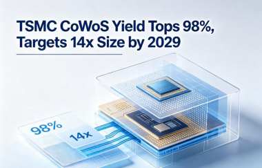
According to TSMC, the company has made further breakthroughs in advanced packaging technology, with its 5.5x reticle size CoWoS (Chip-on-Wafer-on-Substrate) technology entering mass production. TSMC Vice President Kevin Zhang said on August 11 that CoWoS production yields have remained above 98% across multiple AI customer products, with some applications reaching as high as 99%. The company plans to continue introducing new advanced packaging technologies annually and aims to expand CoWoS to 14x reticle size by 2029.
Kevin Zhang, who has been involved in TSMC’s packaging business since the 1990s, said he never expected advanced packaging to experience such rapid growth in recent years. CoWoS, in particular, has become one of the most recognized semiconductor technologies in Taiwan as demand for AI computing continues to accelerate. Zhang joked that introducing himself has become simple: “I’m the CoWoS guy.”
Driven by strong AI demand, TSMC’s CoWoS capacity has nearly doubled every year over the past three years. The company currently operates 10 advanced packaging facilities, with capacity gradually approaching customer demand. Zhang noted that supply has not yet fully met market requirements, but the gap has narrowed significantly.
TSMC’s advanced packaging business has also become an increasingly important contributor to the company’s profitability. Zhang emphasized that the rapid development of CoWoS reflects the growing importance of packaging technologies in the AI semiconductor era.
Beyond CoWoS, TSMC continues to advance its SoIC (System on Integrated Chips) hybrid bonding technology. Zhang said the company’s 6-micron hybrid bonding technology entered high-volume production last year and is expected to achieve a 4.5-micron bonding pitch by 2029, enabling advanced chip stacking solutions such as A14-on-A14 integration. SoIC technology can deliver more than 50 times higher interconnect density and five times better energy efficiency compared with traditional packaging approaches.
Zhang explained that Chiplet architectures not only overcome traditional reticle size limitations but also allow different functional blocks, such as analog and computing components, to be developed separately. This approach can reduce the cost of adopting the latest process technologies while improving overall system performance.
TSMC is also applying advanced algorithms to optimize chiplet integration by matching dies with the most suitable characteristics, enhancing performance consistency at the packaging level. Zhang compared the process to running “the world’s largest online matchmaking service,” where customers provide complex algorithms and TSMC’s global manufacturing network finds the best combination of chiplets before completing assembly and delivery.
With AI workloads driving demand for higher computing performance, TSMC’s continued investment in CoWoS, SoIC, and Chiplet technologies highlights the growing role of advanced packaging as a key foundation for next-generation AI processors.


