
Samsung NRD-K 2 to Produce 2nm HBM Base Dies


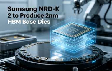
According to South Korean media outlet ZDNet Korea, Samsung Electronics is planning to convert its under-construction NRD-K Line 2 at the Giheung campus from a research-focused facility into a dedicated foundry Send-Fab, aiming to expand its advanced semiconductor manufacturing capacity.
The NRD-K 2 facility is part of Samsung’s large-scale next-generation semiconductor research and development complex, which is designed to secure technological leadership in future chip manufacturing. Samsung plans to invest approximately KRW 20 trillion by 2030 to build three production lines within the complex. The first line was completed at the end of 2024, while preparation for Line 2 began in 2026. The company has already demolished the former Institute of Advanced Technology building at the Giheung campus and started foundation work for the new facility.
Samsung had previously considered using Line 2 as a DRAM mass production facility. However, the company has recently revised the plan and decided to transform it into a dedicated Send-Fab. A Send-Fab serves as a supporting wafer manufacturing facility that receives wafers from other production lines and performs specific critical processes to improve manufacturing flexibility and efficiency.
The main focus of NRD-K Line 2 will reportedly be the production of 2nm-based base dies required for Samsung’s next-generation High Bandwidth Memory (HBM) products, which are expected to be supplied to major customers such as NVIDIA. In an HBM structure, the base die is positioned beneath vertically stacked DRAM layers and plays a crucial role in enabling high-speed data communication between HBM memory and system semiconductors, including GPUs.
As global technology companies continue to accelerate AI infrastructure expansion, demand for advanced HBM solutions is expected to grow significantly. Samsung’s strategy is to apply its most advanced 2nm process technology to future customized HBM products and HBM5 (eighth-generation HBM), helping improve performance and strengthen its competitiveness against rivals. Securing dedicated production capacity at the Giheung campus in advance is considered a key step in Samsung’s strategy to capture future AI semiconductor demand.
Under the latest plan, NRD-K Line 2 is expected to begin operations in the second half of 2028. Due to its relatively limited facility space, adopting a Send-Fab model will allow Samsung to respond more flexibly to advanced semiconductor production needs. However, as the launch date is still about two years away, industry observers believe the facility’s final application could still be adjusted depending on market conditions.
Although the new direction has reportedly been largely finalized internally, Samsung has yet to place equipment purchase orders. Given the rapidly changing semiconductor market environment, the company may continue to fine-tune the investment scale and production strategy based on future demand trends.


