
Samsung Invests ¥40B in Japan AI Chip Packaging R&D Center


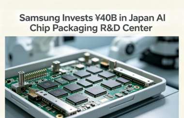
According to reports, Samsung Electronics has established an artificial intelligence (AI) chip packaging research and development center in Yokohama, Japan, with the aim of strengthening cooperation with Japanese companies that have strong expertise in semiconductor back-end processes, including packaging equipment and materials, and accelerating the development of related technologies.
Named the “Samsung Advanced Packaging Lab,” the new R&D facility represents a total investment of 40 billion yen (approximately $257 million), including 22.5 billion yen in support from the Japanese government. Covering approximately 6,600 square meters, the facility will focus primarily on advanced semiconductor back-end processes and packaging technologies.
Reports indicate that Samsung selected Japan for the new R&D center because the country has advanced capabilities across the semiconductor back-end technology sector. As demand for high-bandwidth memory (HBM) continues to grow rapidly with the expansion of AI data centers, semiconductor manufacturers are working to improve the efficiency of connecting multiple chips within a single package, including HBM and graphics processing units (GPUs) responsible for AI computing.
Samsung said that Japanese companies are responsible for producing nearly all of the key materials required for HBM manufacturing. Sumitomo Bakelite holds an estimated 40% share of the global packaging materials market, while Resonac Holdings and Mitsubishi Gas Chemical have strong positions in substrate-related materials.
Establishing an R&D facility in Japan is expected to help Samsung shorten its technology development cycle. Previously, new materials developed in Japan often had to be shipped to South Korea for testing. Regulatory approvals and import and export procedures could sometimes delay the arrival of materials by up to two months. As AI chip technologies continue to evolve rapidly, such delays could affect the competitiveness of semiconductor manufacturers.
Once the Yokohama laboratory becomes fully operational, Samsung will be able to conduct material evaluations and prototype development directly in Japan. Only the most promising technologies are expected to be transferred to Samsung’s production lines in South Korea for mass manufacturing, potentially improving development efficiency and accelerating the commercialization of advanced AI chip packaging technologies.


