
Applied Materials Opens $5B EPIC Center


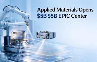
According to Applied Materials, the company officially opened its Equipment and Process Innovation and Commercialization (EPIC) Center on October 12, 2026. Backed by a $5 billion investment, the facility aims to become one of the world's largest collaborative research and development centers for semiconductor process technology and manufacturing equipment, accelerating chip innovation for the artificial intelligence (AI) era.
Located at Applied Materials' Sunnyvale campus in California, the EPIC Center spans 600,000 square feet and includes nearly four acres of advanced cleanroom space. It is designed to bring chipmakers, system companies, equipment partners, and university researchers together with Applied Materials' scientists and engineers to accelerate the development and commercialization of next-generation semiconductor technologies.
Applied Materials President and CEO Gary Dickerson said that growing AI infrastructure and increasingly complex high-performance computing requirements demand closer industry collaboration. The EPIC Center will enable partners to develop new materials, processes, and manufacturing technologies together, helping move innovations into high-volume production faster.
Major semiconductor companies, including TSMC, Intel, Samsung Electronics, Micron, and SK hynix, are among the center's founding partners. Innovation partners include Broadcom, Advantest, SCREEN, Kioxia, and Besi, while research partners include Stanford University, the University of California, Berkeley, and Arizona State University, among others.
TSMC Chairman and CEO C.C. Wei highlighted the importance of collaboration in advancing technologies beyond the 2nm process node, particularly in low-resistance interconnects, advanced packaging, and energy-efficient AI architectures. Intel CEO Lip-Bu Tan also emphasized that closer cooperation with equipment partners will help improve R&D efficiency and accelerate technology development as chip designs become more complex.
Traditionally, semiconductor materials research, equipment development, and process integration have taken place in separate environments, often slowing progress between development stages. The EPIC Center aims to bring these activities together in one facility, allowing partners to test and refine innovations through closer collaboration before introducing them into manufacturing.
Applied Materials expects the center to help chipmakers shorten development cycles, gain earlier access to advanced materials and equipment, and accelerate high-volume manufacturing. For Applied Materials, the collaborative model will provide earlier insight into emerging technology challenges and help guide future R&D investments, supporting the next generation of semiconductor manufacturing.


