
Samsung May Use TSMC’s 3nm Process for NVIDIA HBM


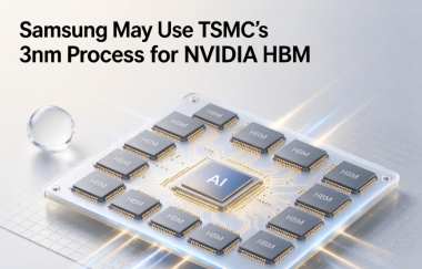
According to a report by South Korea’s Seoul Economic Daily on Sunday, Samsung Electronics plans to use Taiwan Semiconductor Manufacturing Co. (TSMC)’s 3nm process to manufacture base dies for NVIDIA’s next-generation customized high-bandwidth memory (HBM). If confirmed, the move would mark Samsung’s first collaboration with TSMC in HBM manufacturing.
The report, citing industry sources, said NVIDIA had asked Samsung, SK hynix, and Micron Technology to adopt TSMC’s process for the base dies used in NVIDIA’s customized NVHBM, while using sixth-generation DRAM technology for the core dies. Launched in August 2026, NVHBM integrates NVIDIA’s customized memory controller into the base die, aiming to standardize implementation across products from different memory manufacturers.
According to the report, Samsung agreed to NVIDIA’s request following an internal review. However, the company intends to continue manufacturing standard HBM products and customized memory products for other customers using its own processes. Unnamed sources also said Samsung is evaluating whether its in-house foundry business could manufacture NVHBM base dies if demand exceeds TSMC’s available production capacity.


