DIY High-Efficiency Buck Converter with Type-C


Optimizing the Program from the Previous Issue for Better Usability. Developing a Compact and Powerful Spot Welder Utilizing Existing Materials.
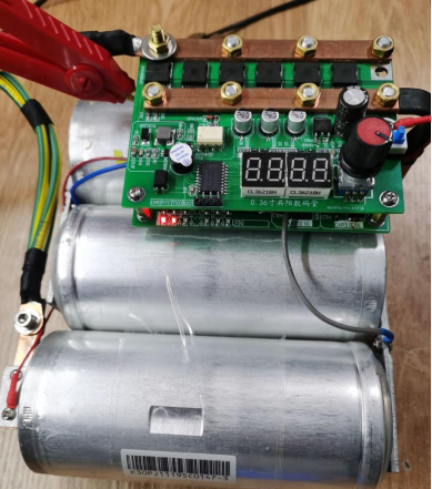
After the previous spot welder was built, it required occasional recharging. The lack of a balancing board made the charging process tedious, as each capacitor had to be charged individually. To address this issue, a new charging balancing board can be developed based on the previous design. By stacking two boards together, significant space can be saved.
I. Setting the Design Requirements
1. Charging Method:
Since the board design allows for 5-12V compatibility, the charging voltage should not be lower than 12V. Using a power adapter would require additional purchases and occupy space, so it is better to pass on that option. A suitable alternative is using a small-sized and commonly available phone charger. Most phone chargers now support fast charging protocols, including 12V output, making Type-C+ protocol triggering the ideal charging method.
2. Voltage Regulation:
Considering the 5-12V universal compatibility of the board, direct input of 12V is not feasible. Voltage regulation is necessary, preferably using a compact and high-efficiency (low heat generation) buck converter circuit.
3. Constant Current Mode:
To prevent damage to the buck converter module when the capacitor's charge is low, a constant current circuit needs to be implemented. Restricting the maximum current to 3A seems reasonable due to limited board size and heat dissipation capabilities. A lower current limit allows for fewer constraints in selecting components.
4. Capacitor Balancing:
Since capacitors are charged in series, different capacitors with varying characteristics will inevitably lead to voltage imbalances. Therefore, a balancing circuit should be designed to monitor the voltage of each capacitor and discharge the ones with excessively high voltage.
II. Component Selection and Circuit Design
1. Triggering the Type-C Protocol:
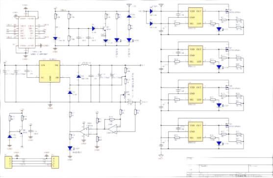
The most convenient option for triggering the Type-C protocol is using an integrated chip with simplified peripheral circuitry. These chips typically support multiple protocols, making them the optimal choice. However, they can be expensive. An alternative is using the popular QC2.0 protocol triggering method, which requires adding an RC timing circuit to ensure the correct power-up sequence. The designed circuit is as follows:

R1 limits the current, triggering DP based on the voltage drop of diode D2 (0.7V).
R2 and R11 form a voltage divider circuit to charge C3 and C4.
D1 acts as a clamp to stabilize the voltage of C3/C4 during the charging process.
After C3 is fully charged, when the voltage on the 1st pin of D1 reaches 1.5V, D1 and Q2 start working.
DN is triggered by the voltage drop across D3.
LED2 indicates power supply status, and LED3 illuminates when the protocol is triggered after VS1 breakdown.
When the Type-C plug is removed, R11 discharges the voltage of C3/C4 in preparation for the next charging cycle.
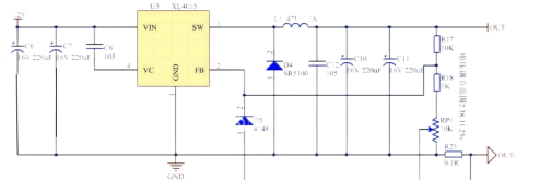
2. Buck Converter Chip Selection:
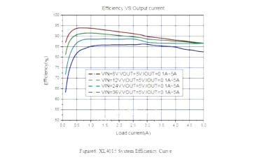
Since the desired output current is 3A, the chosen buck converter chip should have a rated current greater than 3A to meet the design requirements. These chips typically have lower efficiency as the load increases. Therefore, a 5A-rated chip, such as the XL4015E1, is suitable. It offers around 90% efficiency for a 3A output and supports TTL control of the FB pin.
The FB pin is connected to TTL level. When the voltage is above 3.3V, the output is disconnected. When the voltage is below 0.8V, the output is restored. This setup allows for current detection using an operational amplifier, followed by amplification and comparison before being sent to the FB pin to achieve cross flow.
The step-down circuit is configured as follows: R11/R18/RP1 form a voltage regulation circuit, and the output voltage is calculated using the formula VOUT = 1.25 * (1 + R17/R18 + RP1). Since the input is only 12V, the output voltage can only reach around 11.25V.
For the D4 freewheeling diode, a high-current Schottky diode with a voltage rating of 40V is sufficient.
3. Constant current circuit
Because the detected voltage signal has a very low amplitude, directly feeding it into the operational amplifier for judgment would result in a large error. Therefore, a 10x amplification is added. The circuit design is as follows: The voltage drop across R23 is detected, 1A/0.1V, and after tenfold amplification, it becomes 1A/1V. Pin 2 provides a 3V reference voltage. When the current is less than 3A, the operational amplifier outputs a low level, causing D5 to turn off. When the current is greater than 3A, the operational amplifier outputs a high level, causing D5 to conduct forward and disconnect FB, while also lighting up LED7.

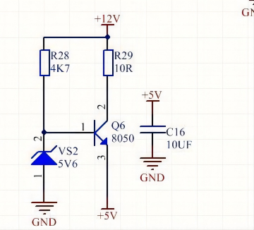
The operational amplifier power supply circuit is as follows: R28 limits the breakdown current of VS2, and R29 limits the current for the 5V power supply.
4. Balancing circuit
The balancing circuit is relatively simple and can be directly implemented using the BW6101 chip dedicated for capacitors. The circuit is as follows: D6/D7 are reverse current protection diodes. The SEL pin is used for selecting the capacitor voltage. When connected to high, it is 2.65V, and when connected to low, it is 2.45V. Q1/R6/R39 form a load discharge circuit. When the voltage exceeds 2.7V, OUT outputs a high level to release the capacitor's energy. The MOSFET used should have a low voltage rating and high current capacity. The schematic actually uses an NMOS transistor salvaged from a computer motherboard, as long as it is in a TO252 package. It is not limited to a specific model.
Schematic Overview:
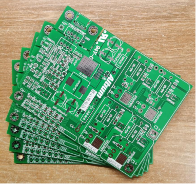
III. PCB Design:
Please note that the BUCK circuit has significant harmonic interference, so the FB signal line should be surrounded by the ground plane. The input and output capacitors should be placed as close as possible to the BUCK chip pins and include decoupling capacitors. The input and output lines should be kept short and thick. The board has several areas with significant heat generation, so a large copper pour should be used to dissipate the heat. The TYPE-C socket should be designed for detachability, making it convenient to connect with other locations using ribbon cables.
IV: Soldering, Debugging, and Errata:
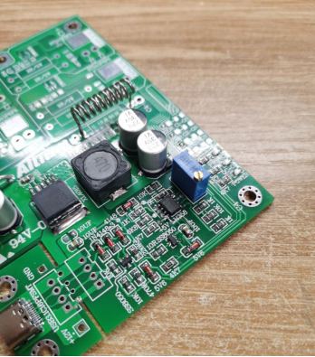
Prepare the components.
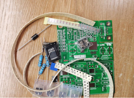

Start by soldering the components as shown in the figure below. Connect a Type-C plug and check if the protocol triggers correctly. Solder C3 for approximately 3 seconds to trigger it; C4 can be left unsoldered.

Type-C Socket Details:

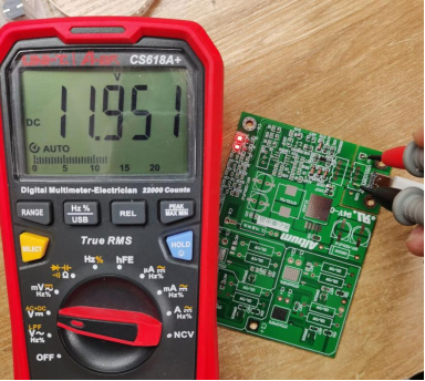
Plug in the Type-C plug, and the POWER light will turn on. After waiting for 3 seconds, the QC2.0 protocol light should also turn on, indicating that the protocol triggering is normal.
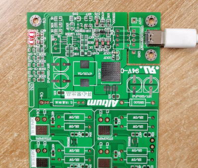
Output voltage is 12V.
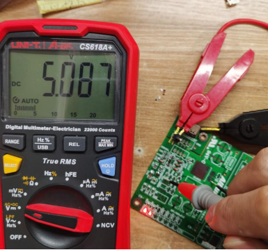
Continue soldering the power supply section of LM358 and test the voltage using the designated 5V test point on the board.
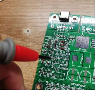
Solder the BUCK circuit section.

Power up and adjust RP1. In my case, since there are 3 capacitors in series, I adjust the voltage to 8V. In reality, it should be slightly higher because the voltage drop across the freewheeling diode needs to be taken into account.
Make a correction to the power supply of LM358 using a jumper wire.
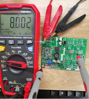
With a load of 2.7A, the circuit achieves constant current (mainly due to resistor value errors in the voltage divider, wire resistance, and amplifier feedback resistor accuracy).
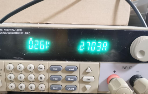
The CC light on the board lights up because the BUCK circuit is operating in an oscillating state after cross flow, and the sound of the inductor is noticeable.

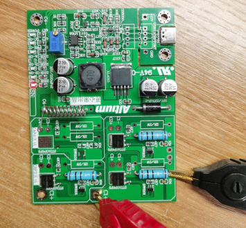
Continue soldering the balancing section. Since only 3 channels are used, C4 can be directly shorted. Solder the C1/C2/C3 parts to complete the section.

Connect C1+/C1- to a voltage of 2.8V. When C1-ON lights up, it indicates that the balancing circuit is functioning, and the other two channels can be debugged in the same way.
Plug in the Type-C connector. Due to the unloaded state, each balancing circuit has a slight conduction.
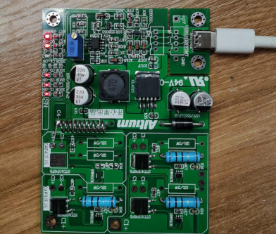
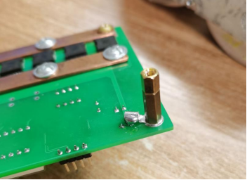
Since there are two midpoints in the series connection of the three capacitors, solder two wires.

Modify the original board by adding a copper pad to make it compatible with this board. The copper pillars are a bit short, so they need to be raised.
Charging with a constant current of 12V is normal.

The input current at 12V is less than 2A, resulting in a power of around 20W. Since the capacitors already have a charge, they reach full capacity in a few minutes. The overall temperature rise of the board is not significant, so the long-term working temperature is estimated to not be too low.

After the current drops below 3A, the CC light goes off, indicating that it has entered constant voltage charging mode.