
Electric bicycles with 60V and 72V use five and six lead-acid batteries (12V/20AH) connected in series for power supply. As the years of use increase, the internal resistance of the six batteries gradually becomes inconsistent, resulting in some batteries charging quickly while others charge slowly. When the charging voltage reaches a certain level, the charger automatically stops charging. At this point, some batteries are overcharged while others are undercharged. Over time, the overcharged batteries may expand, while the undercharged batteries may lose activity, leading to damage to the entire battery pack.
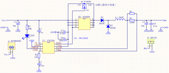
This circuit uses the dedicated CN3768 management chip for 12V batteries to perform three-stage charging of lead-acid batteries. This dedicated management chip is superior to so-called "smart chargers." Only using a dedicated chip for charging management is a true charging circuit. Therefore, you can discard the original 60V or 72V chargers and use this circuit to charge each battery individually. The charging will automatically stop for the battery that is fully charged first, without affecting other batteries. This avoids the drawbacks of series charging and achieves balanced charging.
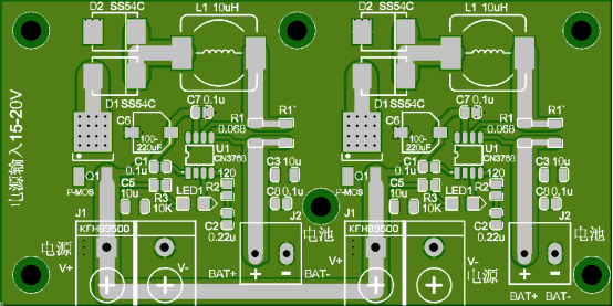
The circuit is designed with two sets of battery charging boards. In practical use, one battery uses one set of circuits on the board. If your electric bicycle has multiple batteries, you will use multiple boards (each board has two sets of charging circuits). As for why the design includes two sets of circuits on one board, it is because it is an experimental circuit that allows simultaneous charging tests for multiple batteries. The power supply output current used is only about 3.5A, while the charging current for two batteries can reach around 3.2A, so it is designed with a maximum of two sets of circuits.
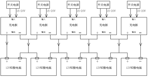
In actual application, one power supply drives one board, and one board charges one battery. If your vehicle has six batteries, you will need 6 power supplies, 6 charging boards, and one set of circuits on each charging board to charge one battery.
Balanced charging schematic:
Schematic diagram:
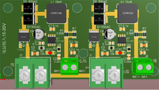
Front view of the PCB:
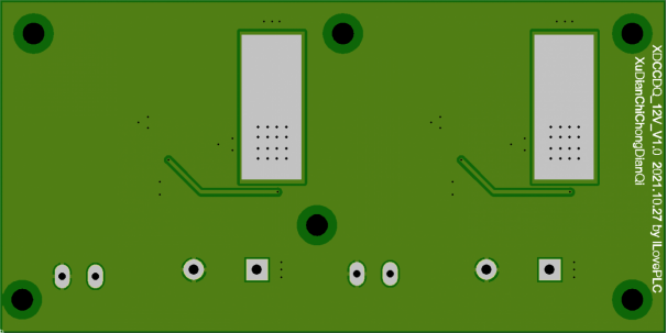
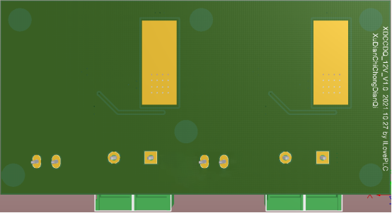
Back view of the PCB:
3D front view image 1:
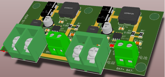
3D front view image 2:
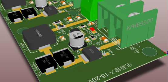
3D front view image 3:
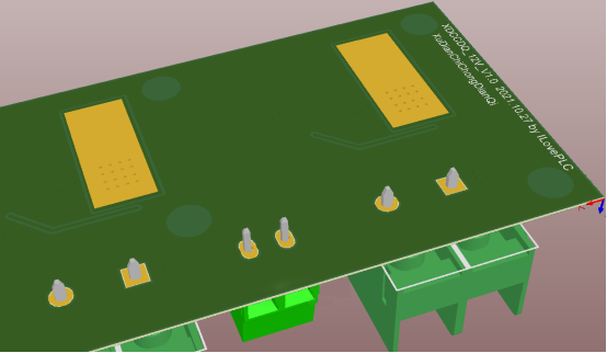
3D back view image 1:
3D back view image 2:
To prevent high current heating, the P-MOS transistor on the PCB has large through holes on the back pads, facilitating the transfer of heat from the MOS transistor to the back copper foil for heat dissipation. The schematic diagram includes two MOS transistors, Q1 and Q2, but in practice, only Q1 is used as it has higher power and better heat dissipation. The schematic diagram also includes two resistors, R1 and R1'. If only one resistor is used, R1 is sufficient with a resistance value of 0.068 ohms. If you need higher current or more precise resistance values, you can use two resistors in parallel. The charging current formula for this circuit is I = 0.12V/R1, where 0.12V is the specified value and cannot be changed. To change the charging current, you can only modify the resistance value of R1.
The schematic diagram shows only one set of charging circuits, while the PCB has two sets of charging circuits, which were duplicated from the first set. Their positive and negative terminals are interconnected. To achieve balanced charging, only one set of circuits should be used; simultaneous use of both sets of circuits is not recommended. Currently, it is in the testing phase, and the success rate is estimated to be high. You can conduct your own board testing to determine the specific results.


