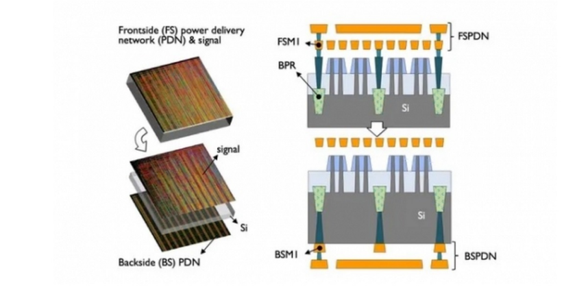
As the trajectory of Moore's Law unfolds, the dimensions of transistors within semiconductor chips continue to shrink, driving up density and necessitating an increasing number of stacked layers. This progression, at times requiring up to 10 to 20 layers of stacking to facilitate power and data signal provision to underlying transistors, has resulted in escalating complexity within the interconnect and power line strata of chips.
Moreover, the downward transmission of electrons precipitates an IR voltage drop phenomenon, causing a reduction in voltage received by chip transistors and consequent performance degradation.
Beyond the issue of power loss, the spatial footprint occupied by power supply lines presents a significant concern. In the intricate routing of power supply lines during later stages of chip fabrication, it often commandeers no less than 20% of available resources. The resolution of contention between signal and power network resources, pivotal for component miniaturization, has emerged as a paramount challenge for chip designers. To counter this challenge, the semiconductor sector is increasingly gravitating towards relocating power supply networks to the rear face of chips.

TSMC's Super PowerRail technology, unveiled within the A16 process, embodies a fusion of super power rail architecture and nanosheet transistor technology. This innovation directly links power transmission lines to source and drain, effectively mitigating voltage drop, streamlining power distribution, facilitating denser chip circuitry packaging, and accommodating an augmented transistor count to bolster computational prowess. Leveraging the A16 process with super power rail technology yields a noteworthy enhancement in computing speed by 8% to 10% compared to N2P at equivalent Vdd (operating voltage), or a commensurate reduction in power consumption by 15% to 20% at identical computing speed. This augmentation in chip density by up to 1.10 times bolsters support for data center products.

Intel's PowerVia technology emerges as another salient solution for backside power delivery. This technology effectuates savings in chip real estate, engendering a more spacious milieu for interconnect layers. By segregating backside power supply lines from interconnect lines and augmenting wire diameter, PowerVia enhances power supply and signal transmission efficacy. Empirical validation of PowerVia technology via Intel's test chips underscores its commendable performance, yielding heightened utilization rates and frequency boosts, while concurrently ameliorating voltage drops and augmenting unit density, thereby potentially curbing costs.

Samsung, a key industry contender, is also making significant inroads in the domain of backside power delivery. In addition to transitioning to GAA transistor technology, Samsung envisages integrating Backside Power Delivery Network (BSPDN) technology into the SF1.4 process by 2027. Compared to conventional front-end power supply networks, Samsung's BSPDN holds promise in reducing wafer area, enhancing overall performance, and mitigating resistance, power consumption, and power transmission constraints. The adoption of these pioneering technologies heralds a watershed moment in mitigating the myriad challenges encountered in modern chip design.


