
In our previous DIY article, DIY: USB2S Adapter Setup Tips & Common Issues, we covered common problems and precautions related to the USB2S adapter — a programmable USB to UART/I2C/SMBus/SPI/CAN/1-Wire converter. In this follow-up, we'll dive into its mechanical dimensions and voltage settings. If you're still interested, keep reading!
1.1 Physical Dimensions
The USB2S module measures 30mm x 45mm (excluding the USB connector). The key sections are shown in the diagram below.
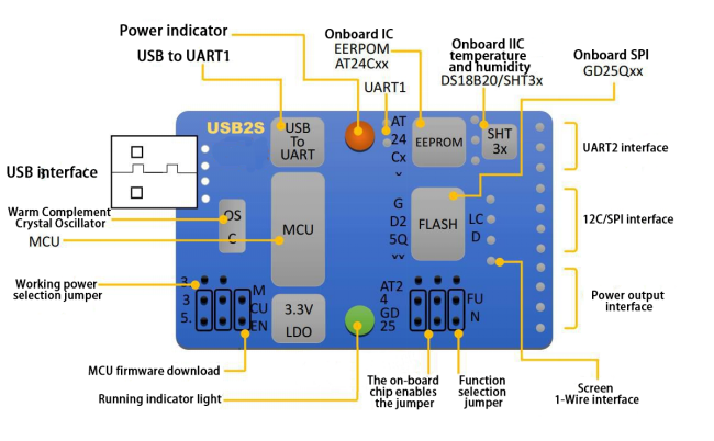
1.2 Structural Composition
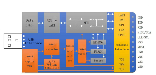
2.1 Power Input
The USB2S is powered through the USB interface, with a voltage input range of 3V to 10V. Unless otherwise specified, the standard USB voltage of 5.0V (VIN = 5.0V) is used by default.
2.2 Setting the Operating Voltage
You can set the USB2S's operating voltage using a voltage selector jumper, as shown in the diagram. If the jumper is on the 3.3V side, the working voltage is 3.3V. If it's on the 5.0V side, the working voltage equals VIN (5.0V when USB-powered).
Important: Both jumpers must be adjusted together to set the correct voltage.
All onboard chips on this module support an operating voltage range of 3.0V to 5.5V. Therefore, if VIN is below 5.5V, you may set the module to either VIN or 3.3V. If VIN exceeds 5.5V, the jumpers must be set to 3.3V to avoid damaging the module.

Note: Except for D+ and D− lines in the USB interface, all digital I/O pins operate at the selected working voltage (VCC/VWK). Before connecting any external device or chip, ensure you select the appropriate working voltage (3.3V or 5.0V) using the jumpers.
2.3 Power Output
Pins 1 to 4 of the external interface provide power output for external devices. The pins are as follows: V50、V33、VCC/VWK、GND.
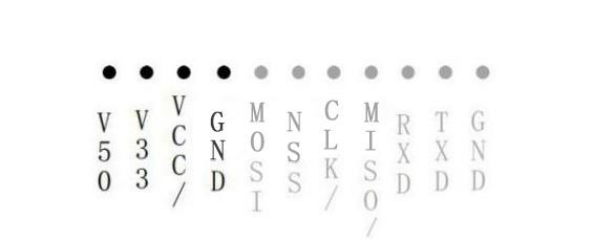
· V50: Outputs the same voltage as VIN (i.e., 5.0V when USB-powered)
· V33: Outputs a regulated 3.3V from VIN
· VCC/VWK: Outputs the selected working voltage (via jumper setting)
The V33 regulator can supply a maximum of 500mA, but it's not recommended to power devices exceeding 300mA.
2.4 I2C Bus
Pins 7 and 8 are used for I2C communication lines — SCL and SDA, respectively. The board includes 2k pull-up resistors. USB2S supports I2C communication speeds from 10kHz to 400kHz. It can operate in both master and slave modes.
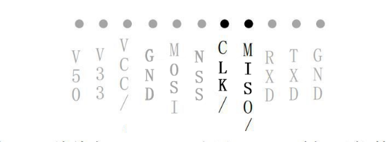
Note: Pins 7 and 8 are shared between the I2C and SPI buses — only one protocol can be used at a time. See Chapter 3 for switching instructions.
The I2C bus is connected to an EEPROM chip and a temperature-humidity sensor chip on the board. These can be enabled via jumper settings in either forced or program-controlled modes.

Jumper Note: The first row of three pins (from left to right) are: VCC, IIC_POW, IO1. If pins 1 and 2 are shorted using a jumper cap, IIC_POW is forced to VCC, powering the onboard I2C chip; If pins 2 and 3 are shorted, IIC_POW connects to IO1, and its power is program-controlled (IO1 high = power on; low = power off).
2.5 SPI Bus
Pins 5, 6, 7, and 8 are used for SPI communication: MOSI, NSS, CLK, and MISO, respectively, CLK and MISO have onboard 2k pull-up resistors.
The SPI interface supports speeds up to 5MHz and supports both master and slave modes, and is compatible with both 3-wire and 4-wire SPI configurations.
Note: Pins 7 and 8 are shared with the I2C bus, so only one interface can be used at a time.
The SPI bus is also connected to an onboard FLASH chip, which can be enabled via jumper settings (forced or program-controlled).
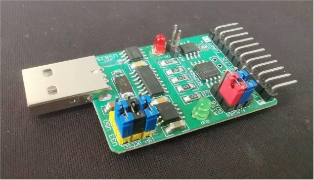
Jumper Note: The second row of three pins (from left to right) are: VCC, SPI_POW, IO2. If pins 1 and 2 are shorted, SPI_POW is forced to VCC, powering the onboard SPI chip; If pins 2 and 3 are shorted, SPI_POW connects to IO2, and its power is program-controlled (IO2 high = power on; low = power off).
Additional Note: IO1 and IO2 also serve as control pins for the onboard SPI Flash chip (GD25Qxx): IO2 acts as HOLD — must be high during operations; if low, SPI signals are ignored, IO1 acts as Write Protect (WP) — must be high to allow write commands; low will restrict the chip to read-only mode.
End.


