In the field of electronic circuit design, selecting the right MOSFET is a critical and complex task. Many engineers face numerous challenges when choosing MOSFETs, and improper selection often results in low circuit efficiency, excessive heat, or even complete failure. This article will explain a practical seven-step selection method in detail and analyze the core challenges and solutions for three specific application scenarios.
What is a MOSFET?
A MOSFET, or Metal-Oxide-Semiconductor Field-Effect Transistor, is a semiconductor device that controls the current through its channel using a gate voltage. It has advantages such as high input impedance, low driving power, and fast switching speed, making it widely used in power control and conversion circuits such as switching power supplies, motor drives, and lighting dimming circuits. MOSFETs are mainly divided into low-voltage and high-voltage types based on their voltage withstand capability.
Low-voltage MOSFETs typically refer to devices with a voltage rating below 100 volts, focusing on low on-resistance and fast switching characteristics. High-voltage MOSFETs, on the other hand, refer to devices rated between 400 volts and 1000 volts or even higher, with designs emphasizing high voltage tolerance and avalanche energy handling capability.
Application Scenarios
However, in practical MOSFET driver designs, engineers often encounter several challenging application scenarios.
The first scenario is low-voltage applications. For example, when the entire system is powered by a 5V supply and a traditional totem-pole circuit drives the MOSFET, the base-emitter voltage drop of the driving transistor, typically around 0.7V, may reduce the actual voltage applied to the MOSFET gate to only 4.3V. In this case, if a MOSFET with a nominal gate threshold voltage of 4.5V is selected, the device cannot fully turn on, operates in the linear region, generates excessive heat, and poses significant risk. This problem is even more pronounced when using lower supply voltages, such as 3.3V.
The second scenario is wide voltage input applications. In these systems, the input voltage is not constant and fluctuates with the load or power grid conditions, causing the PWM controller output driving voltage to vary. To protect the MOSFET gate, many devices integrate a voltage clamp diode to limit the gate-to-source voltage. However, if the driving voltage remains higher than the clamp value, a continuous static current flows through the clamp diode, causing unnecessary power consumption. Simply using a resistive voltage divider to reduce the gate voltage can also result in insufficient gate drive when the input voltage drops, similarly increasing conduction losses.
The third scenario is dual-voltage systems. In modern electronic devices, the logic control section, such as an MCU, often uses 5V or 3.3V, while the power section, such as motors, may use 12V, 24V, or higher voltages. These two power domains usually share a common ground. This requires a driver circuit design that allows low-voltage signals to safely and effectively control high-voltage MOSFETs, while also properly addressing the low-voltage and overvoltage issues that may occur on the high-voltage side.
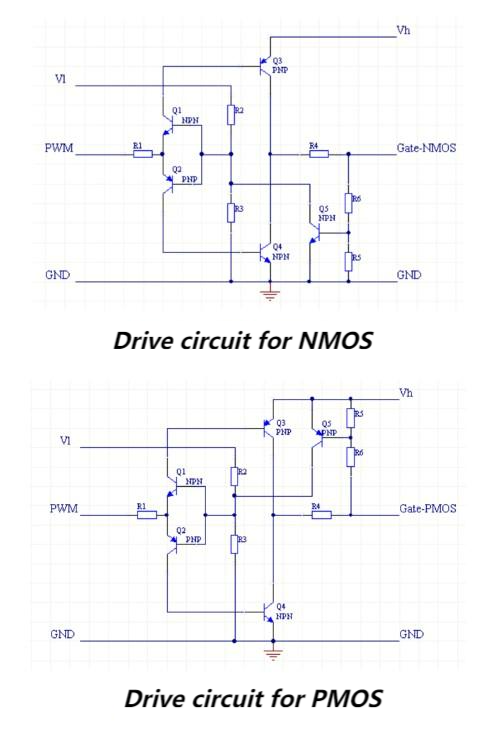
Faced with these three challenges, traditional totem-pole driver structures or many standard MOSFET driver ICs on the market are often inadequate. Here, we share two relatively universal circuits to handle these three application scenarios. The circuit diagram is shown below:

In the diagram, the NMOS and PMOS driver circuits perform the same function; here we only analyze the NMOS driver circuit: Vl and Vh represent the low-side and high-side power supplies, respectively. The two voltages can be the same, but Vl should not exceed Vh.
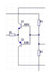
Q1 and Q2 form an inverted totem-pole to provide isolation and ensure that the two driving transistors Q3 and Q4 never conduct simultaneously. R2 and R3 provide a PWM voltage reference, and adjusting this reference allows the circuit to operate in the steeper portion of the PWM waveform.
Q3 and Q4 supply the driving current, and when conducting, the voltage drop relative to Vh and GND is only about one Vce, typically around 0.3V, which is much lower than the standard 0.7V Vce.
R5 and R6 are feedback resistors used to sample the gate voltage, and the sampled voltage is fed through Q5 to strongly provide negative feedback to the bases of Q1 and Q2, thereby limiting the gate voltage to a set value. This value can be adjusted through R5 and R6.
Finally, R1 limits the base current of Q3 and Q4, and R4 limits the gate current of the MOSFETs, i.e., the Ice of Q3 and Q4. If necessary, an acceleration capacitor can be added in parallel with R4.
This circuit provides the following features:
1. It uses a low-voltage supply and PWM to drive high-voltage MOSFETs.
2. It drives MOSFETs with high gate voltage requirements using a small-amplitude PWM signal.
3. It limits the peak gate voltage.
4. It limits input and output currents.
5. It achieves very low power consumption through proper resistor selection.
6. The PWM signal is inverted; NMOS does not require this feature, but it can be solved by adding an inverter beforehand.

A totem-pole consists of two transistors stacked vertically: the upper transistor is NPN, with the collector connected to the positive supply, and the lower transistor is PNP, with the emitter connected to the negative supply, which is ground. The two bases are tied together and connected to the input, and the upper emitter and lower collector are connected
Conclusion
As the circuit analysis above shows, using MOSFETs involves many knowledge points. Correctly selecting MOSFETs is a core part of electronic circuit design, and it is essential to start from understanding the basic parameters. Designers must comprehensively match the supply voltage, load performance, switching frequency, and thermal management requirements for the specific application scenario. Whether in low-voltage, wide-voltage, or dual-voltage systems, one should systematically evaluate voltage rating, conduction characteristics, drive conditions, and peripheral driver circuits to ensure that MOSFETs operate efficiently, safely, and reliably within the design voltage range, thereby improving the overall system performance and reliability.


