
SK hynix Starts $4B U.S. HBM Packaging Plant


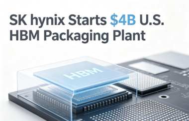
According to SK hynix, the South Korean memory semiconductor manufacturer officially held a groundbreaking ceremony on August 27 at Purdue University’s Holloway Gymnasium in West Lafayette, Indiana, marking the start of construction of its first advanced packaging facility for high-bandwidth memory (HBM) in the United States.
The ceremony attracted significant attention from U.S. government, academic, and industry representatives. Indiana Governor Mike Braun, U.S. Senator Todd Young, and Purdue University President Mitch Daniels attended the event. SK Group was represented by senior executives including Vice Chairman Yoo Jeong-joon, Vice Chairman Lee Hyung-hee, and SK hynix CEO Kwak Noh-jung.
At the ceremony, SK hynix CEO Kwak Noh-jung emphasized the strategic importance of the new facility in supporting the rapidly growing artificial intelligence (AI) industry. He said that simply producing high-performance memory is no longer sufficient in the AI era. The company also needs to develop customized memory solutions for customers’ AI systems and use advanced packaging technologies to maximize the performance of memory, AI chips, and complete computing systems.
SK hynix plans to invest more than $4 billion in the Indiana project. The company expects to complete the facility’s cleanroom construction by October 2028 and begin mass production of next-generation HBM in the second half of 2029. Once fully operational, the site is expected to become a major HBM production hub in the United States, employing more than 1,000 people.
A key feature of the Indiana facility will be its closely integrated manufacturing and technology development network. Advanced wafers produced in South Korea will be shipped to Indiana for advanced packaging and testing. The resulting HBM products manufactured in the United States will then be delivered directly to local customers.
The facility will also include advanced packaging research and testing equipment alongside its production lines. This infrastructure is expected to enable SK hynix to work closely with customers, universities, and industry partners on next-generation packaging technologies, while accelerating prototype development and performance validation.
SK hynix said the investment is already generating a strong supply-chain clustering effect in the region. More than 100 companies involved in semiconductor materials, components, and equipment are currently discussing potential operations in West Lafayette. The company expects this growing industrial ecosystem to support the long-term operation of the Indiana facility while strengthening the local AI and semiconductor ecosystem.
SK hynix estimates that construction and operation of the facility will help create approximately 7,000 direct and indirect jobs in cooperation with U.S. companies.
A U.S. Department of Commerce official attending the ceremony also disclosed that the U.S. government has awarded SK hynix $458 million under the CHIPS and Science Act to support the company’s advanced packaging and research and development initiatives.
In addition, SK hynix and Purdue University signed a memorandum of understanding (MOU) on advanced packaging research during the groundbreaking ceremony. Under the agreement, the two sides will expand academic and R&D collaboration on next-generation system integration and advanced packaging technologies, including HBM.
SK hynix also plans to strengthen partnerships with leading universities and research institutions across the U.S. Midwest. Through these collaborations, the company aims to develop and attract highly skilled semiconductor professionals while accelerating innovation in HBM and advanced semiconductor packaging technologies.


