
Infineon and Wolfspeed Sign 200 mm SiC Wafer Deal


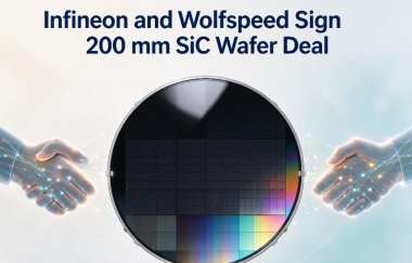
According to Infineon Technologies, the company has signed a multi-year supply agreement with Wolfspeed for 200 mm silicon carbide (SiC) wafers. The agreement marks a transition in their existing supply relationship from 150 mm to 200 mm substrate technology, supporting the development and production of next-generation SiC power semiconductors.
Silicon carbide has become a key enabling technology for electrification and energy efficiency as industries worldwide accelerate the transition toward a lower-carbon economy. Its applications span electric vehicles (EVs), renewable energy systems, industrial power electronics, and power infrastructure for AI data centers.
Alexander Gorski, Chief Operating Officer of Infineon Technologies, emphasized the strategic importance of SiC technology in the energy transition. He noted that ensuring the high quality and reliable supply of 200 mm substrates is essential to fulfilling the company's long-term commitments to customers.
AI data centers are emerging as an important growth driver for SiC power semiconductors. For hyperscale cloud service providers operating large-scale computing infrastructure, power conversion efficiency directly affects operating costs and overall energy consumption. SiC devices offer high switching efficiency and strong thermal performance, making them a viable solution for specific power conversion stages where conventional silicon devices are approaching their practical performance limits.
Beyond AI data centers, the expanding use of SiC technology in electric vehicle powertrains, photovoltaic inverters, and industrial motor drives is strengthening long-term demand for high-quality 200 mm SiC substrates. These applications are creating new opportunities for power semiconductor manufacturers as demand for efficient and reliable energy conversion continues to grow.
Compared with 150 mm wafers, 200 mm SiC wafers offer potential manufacturing cost and productivity advantages. The larger wafer diameter provides more usable chip area per wafer, enabling more semiconductor dies to be produced from each wafer. This can reduce substrate costs per die, improve manufacturing efficiency, and strengthen the economic viability of large-scale SiC power semiconductor production.


