
Apple Develops HMO OLED Technology


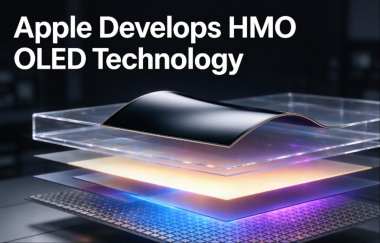
According to industry reports, Apple is developing High-Mobility Oxide (HMO) technology for next-generation Organic Light-Emitting Diode (OLED) panels, with a focus on using existing sputtering processes to reduce manufacturing costs. Although Atomic Layer Deposition (ALD) offers advantages in thin-film precision and material property control, its high equipment and material costs have prompted Apple to evaluate more cost-effective sputtering alternatives.
HMO is being considered as a potential technology for high-resolution OLED displays in premium IT devices, including future MacBook and iMac models. High-end OLED panels currently widely use Low-Temperature Polycrystalline Oxide (LTPO) technology, which combines silicon and oxide semiconductors. If HMO achieves sufficient performance, oxide semiconductors could replace some silicon-based components in the display backplane. This could simplify manufacturing processes and reduce production costs.
Samsung Display is developing sputtering-based HMO technology while also evaluating ALD-based solutions. The company is currently assessing whether the technology can achieve the electron mobility and reliability required by Apple on large-sized substrates. LG Display is also developing sputtering-based HMO technology on its sixth-generation small- and medium-sized OLED production lines, alongside research into ALD processes.
Last year, LG Display demonstrated oxide thin-film transistors (TFTs) fabricated using ALD, achieving electron mobility of approximately 40 cm²/V·s. The company also showcased an OLED sample incorporating these devices. However, given the investment required for additional equipment, LG Display is placing greater emphasis on solutions that can reuse existing sputtering equipment.
Both sputtering and ALD are deposition techniques used to form ultra-thin semiconductor layers in TFT structures. Sputtering uses plasma to bombard a solid target, releasing atoms that subsequently deposit onto a substrate. One of its main advantages is compatibility with existing OLED production equipment. However, achieving both high electron mobility and long-term reliability requires careful optimization of material composition and thin-film structures.
In contrast, ALD uses gaseous precursors to deposit materials layer by layer at the atomic scale. This process enables precise control over film thickness and composition, helping improve the electrical performance and stability of semiconductor layers. However, its higher equipment investment and precursor material costs present challenges for large-scale manufacturing.
As Apple explores HMO technology for future OLED displays, the development efforts of Samsung Display and LG Display highlight the industry's focus on balancing semiconductor performance, manufacturing reliability, and production costs. The choice between sputtering and ALD could play an important role in determining the commercial feasibility of next-generation high-resolution OLED panels.


