
If you're into DIY electronics and want to explore a 24W multi-protocol USB-A charging board, this article is for you.
The complete power center is planned with five different sub-board designs:
1. LM5176 (PD100W)
2. LM3150 (5V 8A 40W) ×2
3. IP6505T (24W) ×3
4. SW3526 (PD65W) + LM25116 (20V 3.25A 65W)
5. PL5501 ×2 (PD65W)
This power supply setup is great for environments prone to power outages. In our previous post—DIY USB Power Hub: LM3150 8A Charging Board—we walked through building the LM3150 module. Today, we’ll be focusing on sub-board #3.
Here's a 3D rendering of the module design:
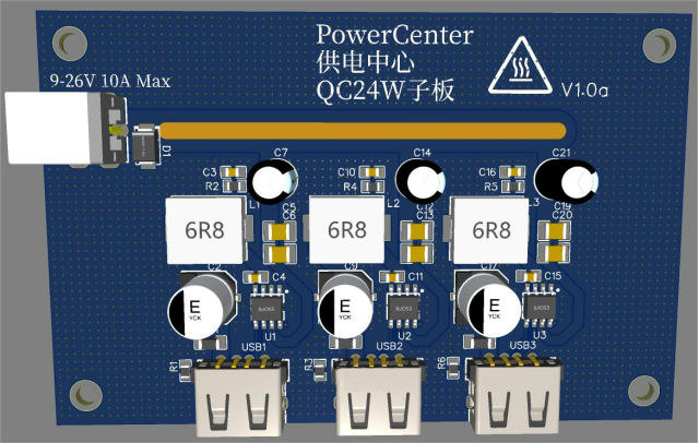
About the chip used this time:
The IP6505T is a synchronous buck converter with an integrated power MOSFET. It supports input voltages from 4.5V to 32V and output voltages from 3V to 12V, with a maximum output power of 24W. It automatically adjusts the output voltage and current based on the fast charging protocol it detects. Typical output profiles include: 4V @ 3.6A, 5V @ 3.4A, 7V @ 3A, 9V @ 2.5A, and 12V @ 2A.
The IP6505T offers up to 97% buck conversion efficiency and supports both CV (constant voltage) and CC (constant current) modes. If the output current is under the threshold, it stays in CV mode, keeping voltage steady. If it exceeds the threshold, it switches to CC mode, reducing voltage accordingly.
It also includes line compensation—when output current increases, the output voltage automatically bumps up slightly to offset cable resistance loss. The soft start feature helps prevent inrush current from destabilizing the input power.
The IP6505T supports a variety of fast charging protocols and uses DP/DM signal lines to auto-detect what protocol the connected device supports, then adjusts output accordingly. Built-in protections include input over-voltage/under-voltage, output over-current, over-voltage, under-voltage, and short circuit protection.
In short, it's a versatile car charger IC that handles both 12V and 24V inputs and supports a wide range of USB-A fast charging protocols. That said, it has a couple of limitations:
· It doesn't support VOOC (IP6505T-Pro does)
· Its SCP protocol has been blocked by newer Huawei phones, limiting power delivery
Fast charging protocols supported:
· BC1.2, Apple, Samsung (5V)
· Qualcomm QC2.0 and QC3.0 (certification ID: 4788120153-2)
· MTK PE1.1/PE2.0
· Huawei FCP
· Huawei SCP (blocked on new devices, lower power)
· Samsung AFC
· Spreadtrum SFCP
Here's a simplified schematic for one of the three identical circuits:

· C5, C6: MLCC input filter capacitors
· C7: Solid-state input filter capacitor
· R2, C3: Snubber circuit at the SW node to absorb spikes and improve EMC
· C4: Bootstrap capacitor for the high-side NMOS driver
· C1: MLCC output filter capacitor
· C2: Aluminum electrolytic output filter capacitor
· R1: Output discharge resistor
As you can see, the peripheral circuitry is relatively simple, thanks to the high level of integration in this chip.
Next, you can move on to making the PCB.
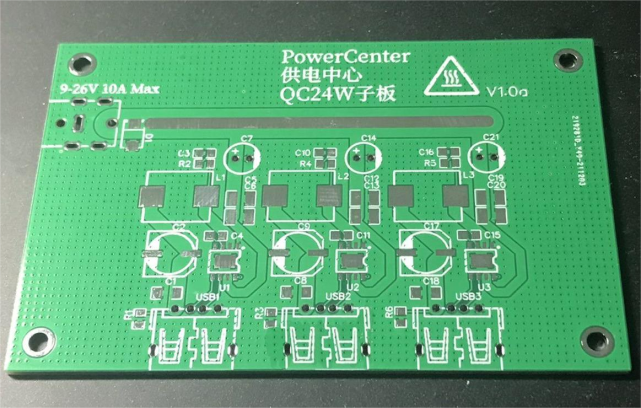
Apply solder paste...
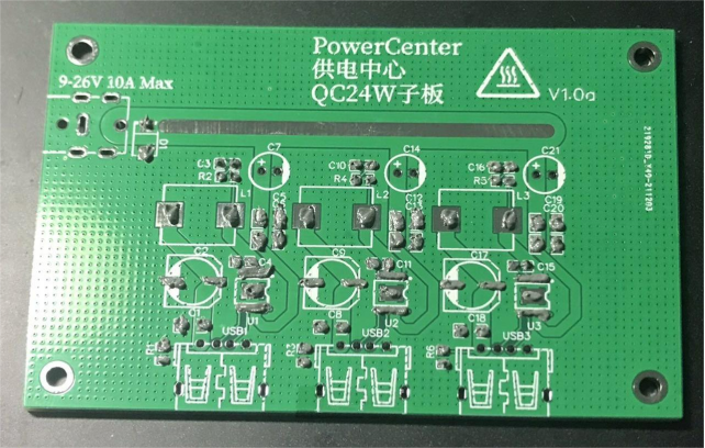
Place the SMD components...
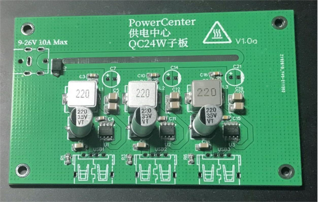
Preheat your hotplate...
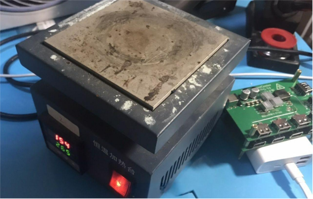
Then place the board on it and gently nudge components into place with tweezers.
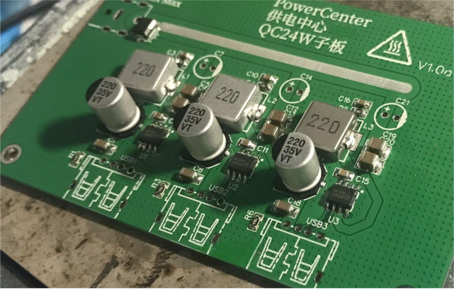
Having all components on the front side offers two main advantages:
1. Easier soldering—just one minute on the hotplate
2. No worries about component conflicts with other stacked sub-boards
Afterward, clean up any solder bridges with a soldering iron and add the through-hole components.
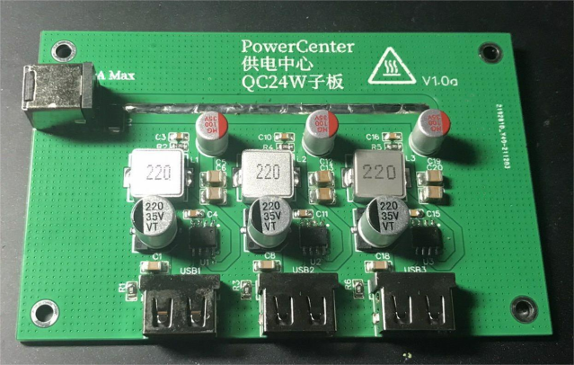
Power it up—static current at 24V is 6mA.
Here's a snapshot of the test results:
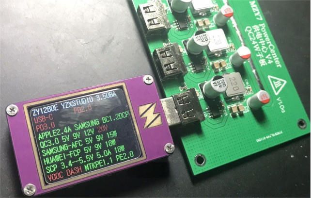
And when charging a power bank:
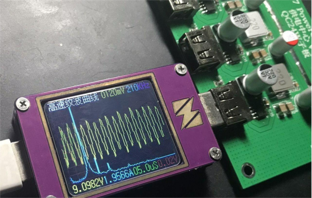
Ripple was a bit high—around 120mV. If that bothers you, try adding more MLCCs and check again.
And that's a wrap.


