
What Causes an SCR to Burn Out?


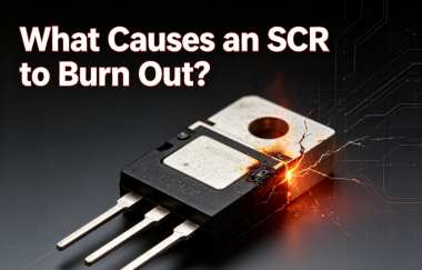
In the electronic components industry, a Silicon Controlled Rectifier (SCR), commonly known as a thyristor, is a widely used power semiconductor device. It is mainly used in power electronic circuits for AC voltage regulation, rectification, power control, and motor control. Because an SCR is designed to handle relatively high voltages and currents, improper component selection, insufficient heat dissipation, or abnormal voltage and current surges during operation can cause overheating, breakdown, or even burnout. Understanding the causes of SCR burnout and taking appropriate protective measures are important for improving circuit stability and extending component service life.
Catalog
III. Basic Structure of an SCR
I. What Is an SCR?
A Silicon Controlled Rectifier (SCR) is a semiconductor device with unidirectional conduction and controllable turn-on characteristics. A typical SCR has three terminals: the anode (A), cathode (K), and gate (G). Under normal conditions, the SCR remains in the blocking state. When a forward voltage is applied between the anode and cathode and an appropriate trigger signal is applied to the gate, the device switches from the off state to the conducting state.
It should be noted that an SCR is not simply a “bidirectional switch.” A conventional SCR provides unidirectional conduction, while bidirectional AC control is generally implemented using devices such as a Triode for Alternating Current (TRIAC). Therefore, when selecting an SCR or analyzing the causes of burnout, its voltage, current, and gate trigger parameters should be evaluated according to the specific device datasheet.
II. How Does an SCR Work?
An SCR uses a four-layer PNPN semiconductor structure. When the anode is positively biased relative to the cathode, the SCR normally remains in the blocking state rather than turning on immediately. When the gate receives a trigger current that meets the specified requirements, a regenerative positive-feedback process occurs inside the device, causing the SCR to rapidly enter the conducting state.
Once the SCR turns on, the gate generally does not need to receive continuous trigger current. As long as the anode current remains above the holding current, the device continues to conduct. In DC circuits, the SCR generally needs to be turned off by reducing the current below the required level or by using a dedicated commutation circuit. In AC circuits, the current normally decreases around the zero-crossing point, allowing the SCR to naturally return to the blocking state.
III. Basic Structure of an SCR
A conventional SCR consists of four alternating P-type and N-type semiconductor layers, forming a PNPN structure, with three main terminals: the anode (A), cathode (K), and gate (G). This internal structure gives the SCR relatively high voltage withstand capability and strong current-handling capability. At the same time, the device has specific requirements for gate trigger current, forward voltage, reverse voltage, and transient surges.
In practical circuit design, engineers should pay close attention to the parameters specified in the SCR datasheet, including repetitive peak off-state voltage, repetitive peak reverse voltage, average on-state current, peak on-state current, gate trigger current, and junction temperature. An SCR should not be selected solely according to its rated current.
IV. Causes of SCR Burnout
1. Breakdown caused by excessive voltage. When the voltage across an SCR exceeds its rated voltage withstand capability in either the forward or reverse direction, the internal PN junctions may break down. In particular, inductive loads such as motors, transformers, and relays can generate transient voltage spikes during switching. Without adequate snubber or clamping protection, these voltage spikes may damage the SCR.
2. Overcurrent causing excessive heating. When the load current exceeds the SCR's rated operating range, power losses in the device increase significantly. Continuous overcurrent can cause the junction temperature to rise rapidly, eventually resulting in chip damage, package failure, or even a short-circuit failure. Excessive inrush current during startup is also a common cause of SCR damage.
3. Insufficient heat dissipation. An SCR generates a certain amount of on-state power loss while conducting, and this electrical energy is ultimately converted into heat. If the heatsink is undersized, installed improperly, exposed to excessive ambient temperatures, or affected by obstructed cooling airflow, the junction temperature may exceed the allowable limit. Long-term operation at high temperatures accelerates device aging and increases the risk of thermal failure.
4. Excessive rates of voltage and current change. SCRs have specified limits for dv/dt and di/dt. An excessively high rate of voltage rise may cause unwanted turn-on, while an excessive rate of current rise can result in localized current concentration within the chip and severe local heating. Therefore, these two parameters require particular attention in high-speed switching circuits and circuits with inductive loads.
5. Improper gate trigger circuit design. Insufficient gate trigger current, unstable trigger pulses, or abnormal interference affecting the gate may prevent the SCR from turning on reliably. An unstable operating condition can increase device losses and consequently raise the risk of overheating and damage.
V. How to Prevent SCR Burnout
First, the SCR should be selected according to the actual operating voltage, load current, startup inrush current, and operating frequency, with sufficient voltage and current margins. For inductive loads, appropriate transient protection circuits, such as RC snubbers and varistors, can be added according to the application to reduce the impact of voltage spikes on the SCR.
Second, proper thermal management is essential. A suitable heatsink should be selected based on the SCR's power dissipation, ambient temperature, and maximum allowable junction temperature. The device should also be properly mounted to ensure good thermal conduction between the SCR and heatsink. For high-power applications, additional cooling methods such as forced-air cooling may be required to prevent prolonged operation at excessive temperatures.
In addition, the gate drive circuit should be properly designed to ensure that the trigger current, trigger voltage, and pulse width meet the device specifications while minimizing electromagnetic interference. For loads that may generate high inrush currents, additional protection measures such as fuses and current-limiting circuits can be used to further reduce the risk of permanent SCR damage.
VI. Conclusion
SCR burnout is commonly associated with overvoltage, overcurrent, insufficient heat dissipation, excessive dv/dt or di/dt, and abnormal gate triggering. In practical electronic circuit design, engineers should consider not only the SCR's rated current but also its voltage rating, inrush current capability, junction temperature, gate trigger parameters, and load characteristics. Through proper SCR selection, effective thermal management, transient and surge protection, and optimized gate drive design, the risk of SCR burnout can be significantly reduced, improving the reliability and long-term stability of power electronic systems.


