
Continuing from the previous two DIY guides: DIY Guide: Convert GREENTEK GU10 to E27 Spotlight and DIY GuideⅡ: Low-Voltage Spotlight Programme Design, this article will delve into the corresponding circuit design. Let's start from the input.
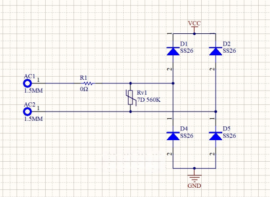
As mentioned before, SS26 forms a bridge rectifier circuit, with a varistor and a fuse providing overvoltage protection (the zero-ohm resistor shown in the diagram is actually a 1206 surface-mount fuse). During the design process, we deliberated between using a one-time fuse and a resettable fuse. One-time fuses have fast response but are irreversible, while resettable fuses are reversible but have slower response times and lower withstand voltage for high currents.
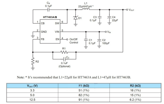

The DC-DC step-down circuit is employed to power the touch chip. The circuit prototype is almost copied verbatim, with the addition of two 47uF MCLL capacitors at the output to reduce ripple and ensure the reliable operation of the touch chip. Whether two capacitors are necessary will depend on the actual performance during testing.
Apart from filtering capacitors, the feedback loop also influences circuit ripple and stability. As seen in the circuit diagram, it's crucial to take feedback from behind the filtering capacitors. Some chip datasheets depict the feedback resistor in front of the filtering capacitors for ease of understanding. Additionally, the choice of feedback resistor value requires careful consideration.
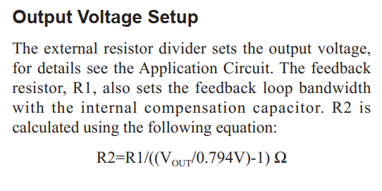
Since resistor values have a specific range, they should be in the same order of magnitude as typical circuit resistances. Refer to the diagram below:
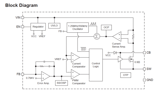
The principle behind feedback involves balanced amplification. Anyone familiar with operational amplifier circuits understands the concept of balanced resistors. To match the impedance of external voltage divider resistors with the internal reference voltage, they should have a similar impedance to the in-phase terminal impedance, enhancing circuit stability.
Next up is the touch control and LED driver circuits.
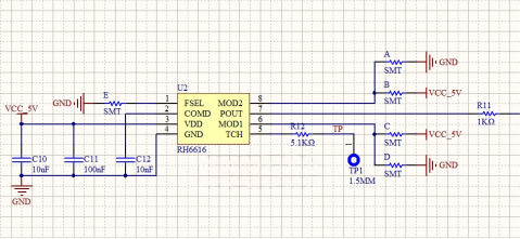
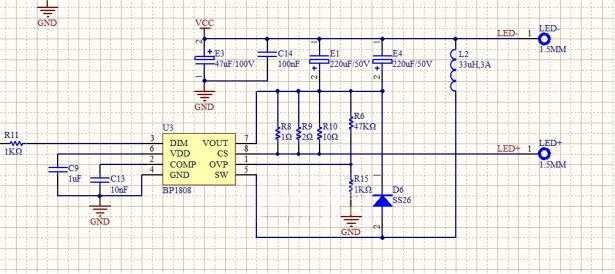
Again, these circuits are nearly identical to the typical circuits found in manuals. The four control modes of the touch chip are determined by the high or low logic levels of two MODE pins. Here, we designed them as solder pads for ease of assembly and cost reduction. The constant current value of the LED driver circuit is determined by three resistors, R8, R9, and R10. The CS pin maintains a fixed voltage of 0.2V, consistent with the original circuit. Therefore, the values of the three resistors are the same as the original circuit, and the current can be adjusted by altering resistor values. Two low ESR electrolytic capacitors with a capacitance of 220uF are used for LED filtering. As mentioned earlier, the PB1808 datasheet recommends a 1uF or larger MLCC capacitor for output filtering. However, due to the low dimming frequency of the touch chip at 4KHz, which leads to significant ripple voltage and audible noise from MCLL, we opted for electrolytic capacitors. Although the capacitance value is the same as that in the original circuit, the driving scheme is different, so the specific ripple voltage remains to be tested.
With the schematic design completed, it's time to lay out the board.
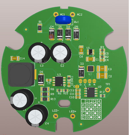
The dimensions of the circuit board must be measured using calipers. All components are placed on the top layer. The power input is at the top, LED driver output at the bottom, LED driver circuit on the left, and touch chip power supply and driver on the right.
Top layer schematic, focusing on the switching power supply circuit, requires attention to the main loop of input and output due to the large pulse current, usually necessitating extensive copper grounding. Additionally, ensure proper heat dissipation for the DC-DC chip, ideally with large-area grounding copper on the same layer as the solder pads. The touch chip's touch sensing foot should have short leads, and wire diameter and distance from the copper should follow the specifications, with TP points soldered to the touchpad.
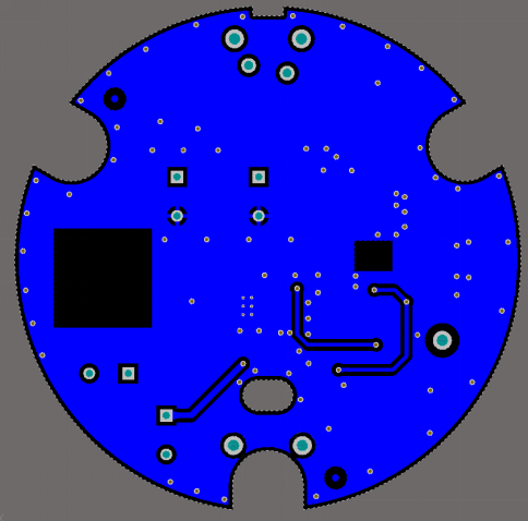
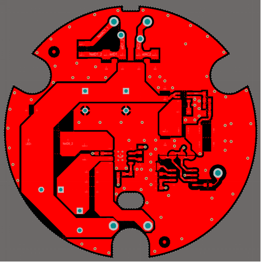
Bottom layer schematic. You can clearly see two black squares, indicating that the copper beneath two inductors has been dug out. This is purported to reduce interference in the ground plane. However, this assertion is controversial. The argument for digging out suggests that there's significant pulsating current on the inductors, which induces signal coupling to the bottom layer ground plane. Conversely, others argue that the coupling energy of the inductors is weak and only affects a small area directly below, so digging it out would compromise the integrity of the ground plane. Considering the board's overall design, we opted to dig out the ground.
With that, the circuit design is essentially complete. The rest is up to you to attempt soldering and debugging.


